- 您现在的位置:买卖IC网 > Sheet目录323 > DS3045W-100# (Maxim Integrated)IC NVSRAM 1MBIT 100NS 256BGA
�� �
�
�3.3V� Single-Piece� 1Mb� Nonvolatile� SRAM�
�with� Clock�
�SRAM� Read� Mode�
�The� DS3045W� executes� an� SRAM� read� cycle� whenever�
�CS� (RTC� chip� select)� and� WE� (write� enable)� are� inactive�
�(high)� and� CE� (SRAM� chip� enable)� is� active� (low).� The�
�unique� address� specified� by� the� 17� address� inputs� (A0�
�to� A16)� defines� which� of� the� 131,072� bytes� of� SRAM� data�
�is� to� be� accessed.� Valid� data� will� be� available� to� the�
�eight� data� output� drivers� within� t� ACC� (access� time)� after�
�the� last� address� input� signal� is� stable,� providing� that� CE�
�and� OE� (output� enable)� access� times� are� also� satisfied.�
�If� CE� and� OE� access� times� are� not� satisfied,� then� data�
�access� must� be� measured� from� the� later� occurring� sig-�
�nal� (� CE� or� OE� )� and� the� limiting� parameter� is� either� t� CO� for�
�CE� or� t� OE� for� OE� rather� than� address� access.�
�SRAM� Write� Mode�
�The� DS3045W� executes� an� SRAM� write� cycle� whenever�
�CS� is� inactive� (high)� and� the� CE� and� WE� signals� are�
�active� (low)� after� address� inputs� are� stable.� The� later-�
�occurring� falling� edge� of� CE� or� WE� determines� the� start� of�
�the� write� cycle.� The� write� cycle� is� terminated� by� the� earlier�
�rising� edge� of� CE� or� WE� .� All� address� inputs� must� be� kept�
�valid� throughout� the� write� cycle.� WE� must� return� to� the�
�high� state� for� a� minimum� recovery� time� (t� WR� )� before�
�another� cycle� can� be� initiated.� The� CS� and� OE� control�
�signal� should� be� kept� inactive� (high)� during� SRAM� write�
�cycles� to� avoid� bus� contention.� However,� if� the� output� dri-�
�vers� have� been� enabled� (� CE� and� OE� active)� then� WE� dis-�
�ables� the� outputs� in� t� ODW� from� its� falling� edge.�
�Clock� Operations�
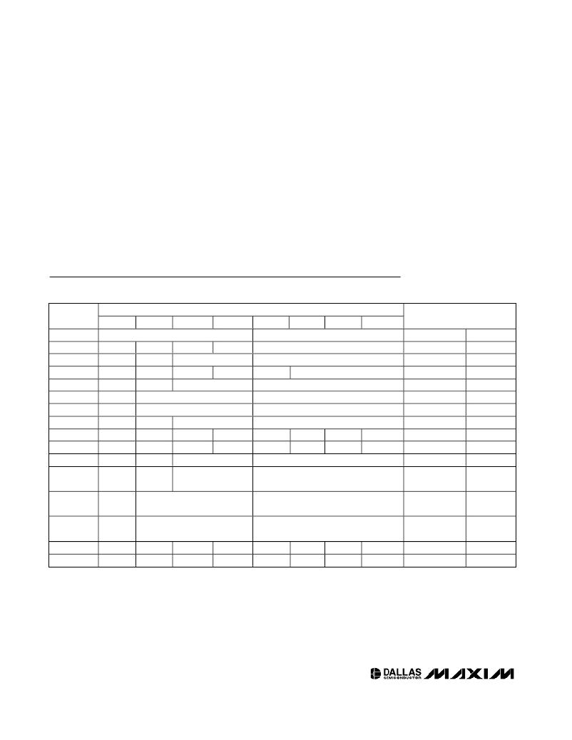
�Table� 2.� RTC� Register� Map�
�ADDRESS�
�B7�
�B6�
�B5�
�B4�
�DATA�
�B3�
�B2�
�B1�
�B0�
�FUNCTION/RANGE�
�xxxxFh�
�10� YEAR�
�YEAR�
�YEAR�
�00� –� 99�
�xxxxEh�
�xxxxDh�
�X�
�X�
�X�
�X�
�X�
�10� M�
�10� DATE�
�MONTH�
�DATE�
�MONTH�
�DATE�
�01� –� 12�
�01� –� 31�
�xxxxCh�
�xxxxBh�
�X�
�X�
�FT�
�X�
�X�
�10� HOUR�
�X�
�X�
�DAY�
�HOUR�
�DAY�
�HOUR�
�01� –� 07�
�00� –� 23�
�xxxxAh�
�xxxx9h�
�X�
�OSC�
�10� MINUTES�
�10� SECONDS�
�MINUTES�
�SECONDS�
�MINUTES�
�SECONDS�
�00� –� 59�
�00� –� 59�
�xxxx8h�
�W�
�R�
�10� CENTURY�
�CENTURY�
�CONTROL�
�00� –� 39�
�xxxx7h�
�xxxx6h�
�WDS�
�AE�
�BMB4�
�Y�
�BMB3�
�ABE�
�BMB2�
�Y�
�BMB1�
�Y�
�BMB0�
�Y�
�RB1�
�Y�
�RB0�
�Y�
�WATCHDOG�
�INTERRUPTS�
�?�
�?�
�xxxx5h�
�xxxx4h�
�xxxx3h�
�xxxx2h�
�AM4�
�AM3�
�AM2�
�AM1�
�Y�
�Y�
�10� DATE�
�10� HOURS�
�10� MINUTES�
�10� SECONDS�
�DATE�
�HOURS�
�MINUTES�
�SECONDS�
�ALARM� DATE�
�ALARM�
�HOURS�
�ALARM�
�MINUTES�
�ALARM�
�SECONDS�
�01� –� 31�
�00� –� 23�
�00� –� 59�
�00� –� 59�
�xxxx1h�
�xxxx0h�
�Y�
�WF�
�Y�
�AF�
�Y�
�0�
�Y�
�BLF�
�Y�
�0�
�Y�
�0�
�Y�
�0�
�Y�
�0�
�UNUSED�
�FLAGS�
�?�
�?�
�x� =� Don’t� care� address� bits.�
�X� =� Unused.� Read/writeable� under� write� and� read� bit� control.�
�FT� =� Frequency� test� bit.�
�OSC� =� Oscillator� start/stop� bit.�
�W� =� Write� bit.�
�R� =� Read� bit.�
�WDS� =� Watchdog� steering� bit.�
�BMB0–BMB4� =� Watchdog� multiplier� bits.�
�RB0,� RB1� =� Watchdog� resolution� bits.�
�AE� =� Alarm� flag� enable.�
�Y� =� Unused.� Read/writeable� without� write� and� read� bit� control.�
�ABE� =� Alarm� in� backup� mode� enable.�
�AM1–AM4� =� Alarm� mask� bits.�
�WF� =� Watchdog� flag.�
�AF� =� Alarm� flag.�
�0� =� Reads� as� a� 0� and� cannot� be� changed.�
�BLF� =� Battery� low� flag.�
�12�
�____________________________________________________________________�
�发布紧急采购,3分钟左右您将得到回复。
相关PDF资料
DS3050W-100#
IC NVSRAM 4MBIT 100NS 256BGA
DS3065W-100#
IC NVSRAM 8MBIT 100NS 256BGA
DS3065WP-100IND+
IC SRAM 3.3V 8MB 34POWERCAP MOD
DS3070W-100#
IC NVSRAM 16MBIT 100NS 256BGA
DS321X
KIT X-WIDE DESIGN STRIP VERT
DS323X
KIT X-WIDE DESIGN STRIP VERT
DS87001-E52
ADAPTER MCU 52-TQFP TO 40-DIP
DS89C450-K00
EVAL KIT FOR DS89C450
相关代理商/技术参数
DS30506
制造商:VISHAY 制造商全称:Vishay Siliconix 功能描述:Ultra-Small Leadless Surface Mount Package
DS3050W
制造商:MAXIM 制造商全称:Maxim Integrated Products 功能描述:3.3V Single-Piece 4Mb Nonvolatile SRAM with Clock
DS3050W-100
功能描述:NVRAM
RoHS:否 制造商:Maxim Integrated 数据总线宽度:8 bit 存储容量:1024 Kbit 组织:128 K x 8 接口类型:Parallel 访问时间:70 ns 电源电压-最大:5.5 V 电源电压-最小:4.5 V 工作电流:85 mA 最大工作温度:+ 70 C 最小工作温度:0 C 封装 / 箱体:EDIP 封装:Tube
DS3050W-100#
功能描述:NVRAM
RoHS:否 制造商:Maxim Integrated 数据总线宽度:8 bit 存储容量:1024 Kbit 组织:128 K x 8 接口类型:Parallel 访问时间:70 ns 电源电压-最大:5.5 V 电源电压-最小:4.5 V 工作电流:85 mA 最大工作温度:+ 70 C 最小工作温度:0 C 封装 / 箱体:EDIP 封装:Tube
DS30519
制造商:DIODES 制造商全称:Diodes Incorporated 功能描述:2.0A SURFACE MOUNT SCHOTTKY BARRIER RECTIFIER
DS305710A
制造商:Amphenol Corporation 功能描述:
DS305710A(621)
制造商:Amphenol Corporation 功能描述:
DS305712A
制造商:Amphenol Corporation 功能描述: